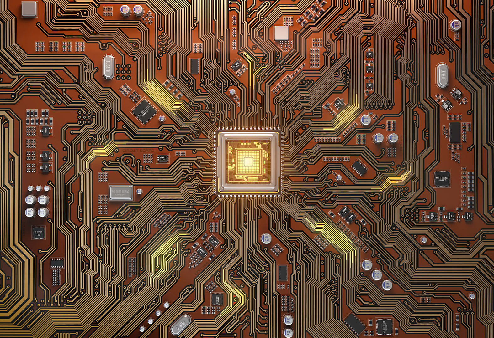
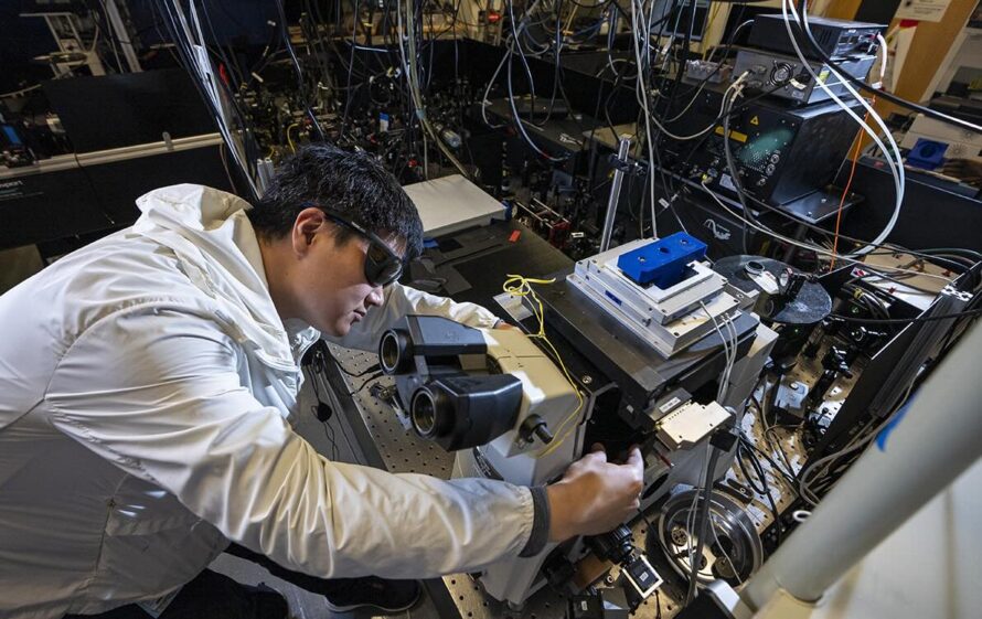
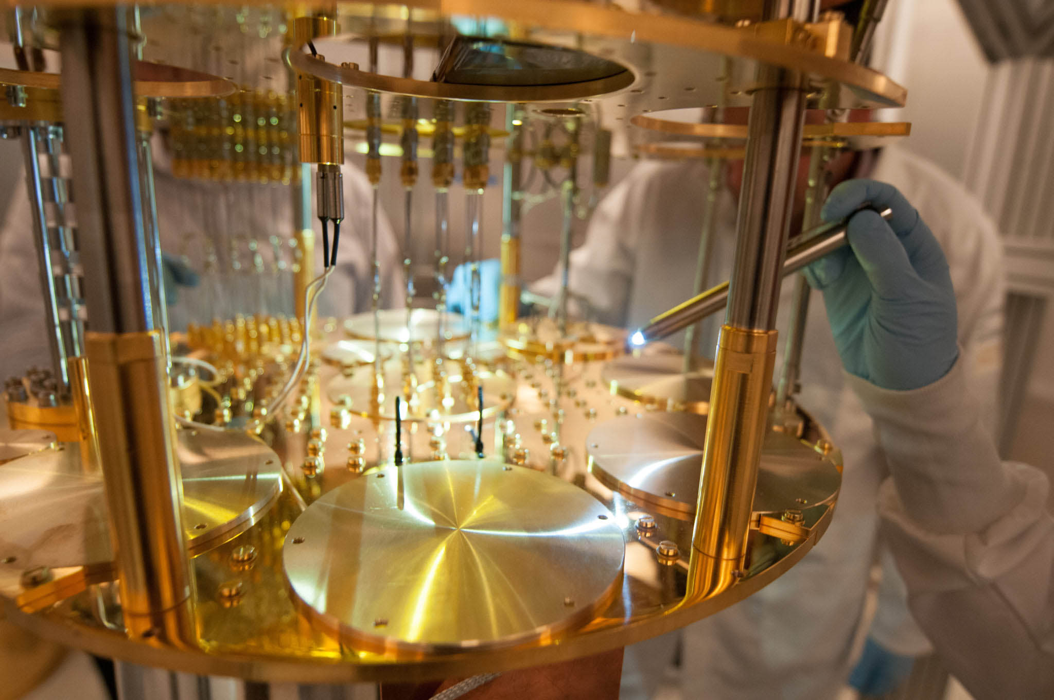
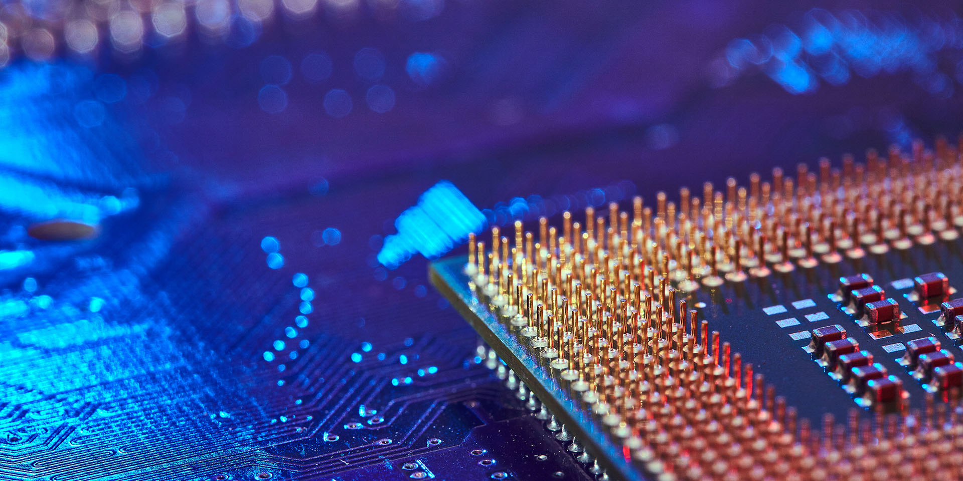
Microelectronics are shaping the modern world. Berkeley Lab brings together deep scientific expertise, advanced facilities, and public-private partnerships to tackle fundamental challenges and reimagine the future of computing.

Center for X-ray Optics (CXRO)
Developing EUV systems to address national needs in health, the environment, and semiconductor manufacturing.
Center for High Precision Patterning Science (CHiPPS)
Creating a fundamental understanding and control of patterning processes for advanced manufacturing of future-generation microelectronics.
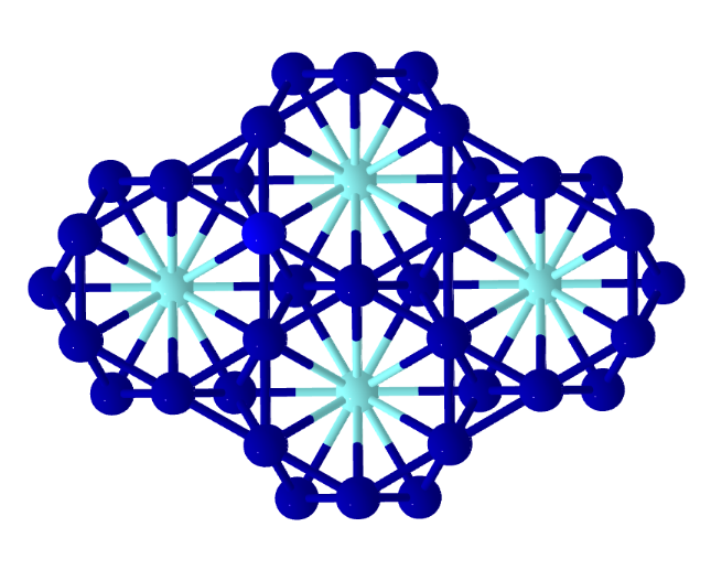
Quantum Materials Program

Investigating next-generation quantum materials to understand and control new electronic behavior.
Nanoscale Hybrids: A New Paradigm for Energy-Efficient Microelectronics
Part of the DOE’s Microelectronics Energy Efficiency Research Center for Advanced Technologies (MEERCAT).
Microscopic and Electronic STRucture Observatory (MAESTRO) beamline

Dedicated to determining the electronic structure of materials at the mesoscopic (10–100 nm) scale.
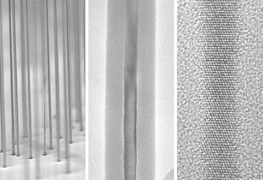
Co-design of Ultra-Low-Voltage Beyond CMOS Microelectronics
Exploring new physics leading to higher energy efficiency in computing.
Electronic Materials Program

Developing novel semiconductor materials for advanced electronic applications.
Intelligence Advanced Research Projects Activity (iARPA) AGILE
Reinventing computer architecture to efficiently handle complex, dynamic data, enabling better analysis and predictions from massive datasets and unlocking new levels of computing performance.
PARADISE++

Building a large-scale HPC framework to simulate post-Moore architectures built using emerging technologies.
Adaptive mesh Refinement Time-domain ElectrodynaMics Solver (ARTEMIS)
A full physical electromagnetic simulation framework for modeling next-generation microelectronics.
Advanced technologies research at the National Energy Research Scientific Computing Center (NERSC)
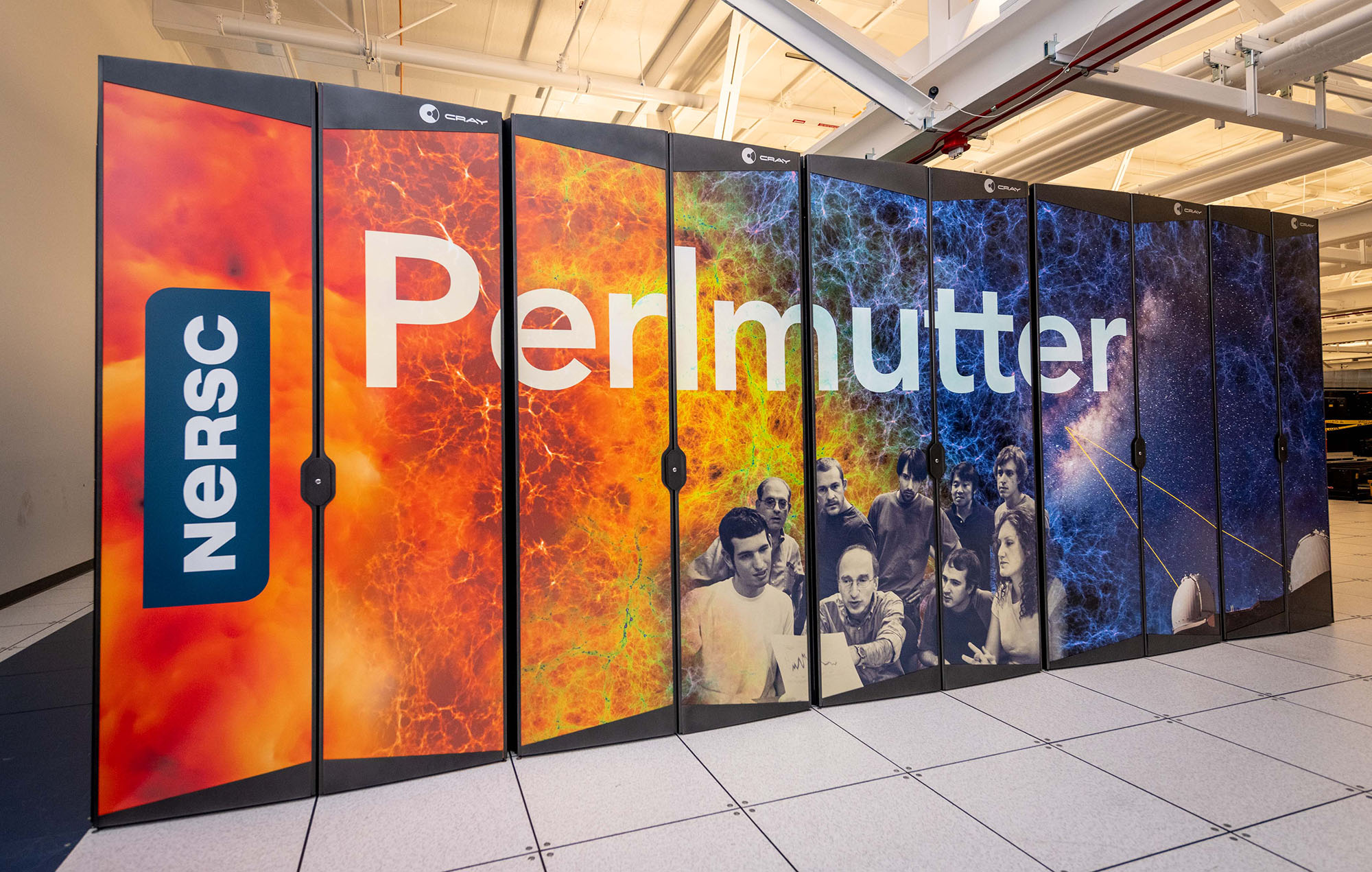
Enabling and supporting the development of next-generation HPC platforms and applications.
The Materials Project
Accelerating innovation in materials research for batteries, energy materials, and computer chips.
We foster strong partnerships that guide innovations from the Lab toward the marketplace. See our microelectronics technologies.

"The mission of the CHiPPS center is to create new fundamental understanding and control of patterning materials and processes with atomic precision. The goal is to enable the large-scale manufacturing of next-generation microelectronics."

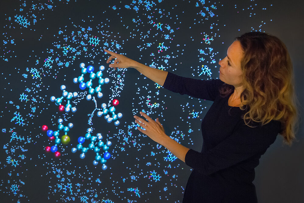
"Our work shows that we need to go beyond the analogy of Lego blocks to understand devices made from stacks of disparate atomically-thin, two-dimensional materials. The seemingly distinct layers communicate through shared electronic pathways, allowing us to access and eventually design functionalities that are greater than the sum of the parts."

"We are interested in the topology of various photonic systems. We developed one of the first models that allow the understanding of the twist degree of freedom in moiré photonic structures and the prediction of novel optical properties in such systems."
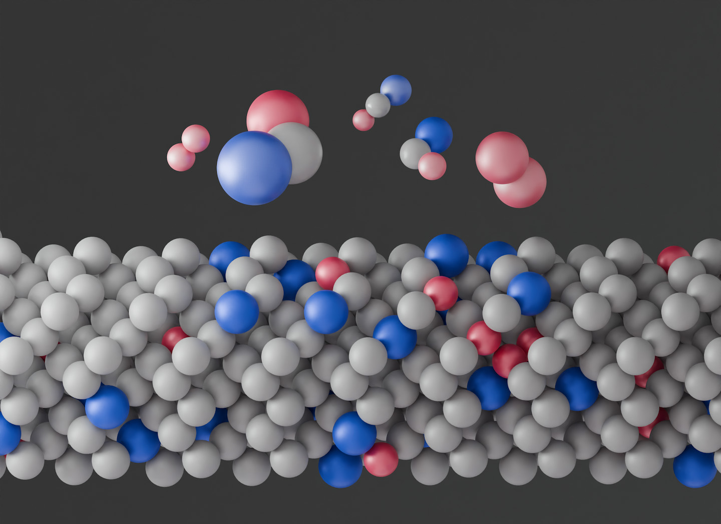
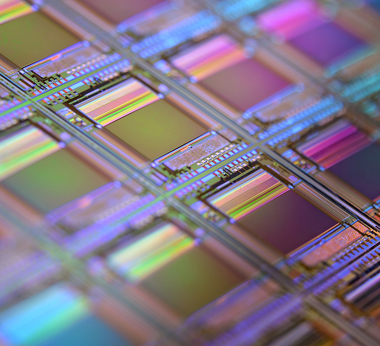
Inside the microchips powering your devices, the atoms have a hidden order all their own. Berkeley Lab scientists have confirmed that elements in semiconductors have preferred arrangements that impact the material’s properties, opening the door for new fabrication methods and unique technologies.
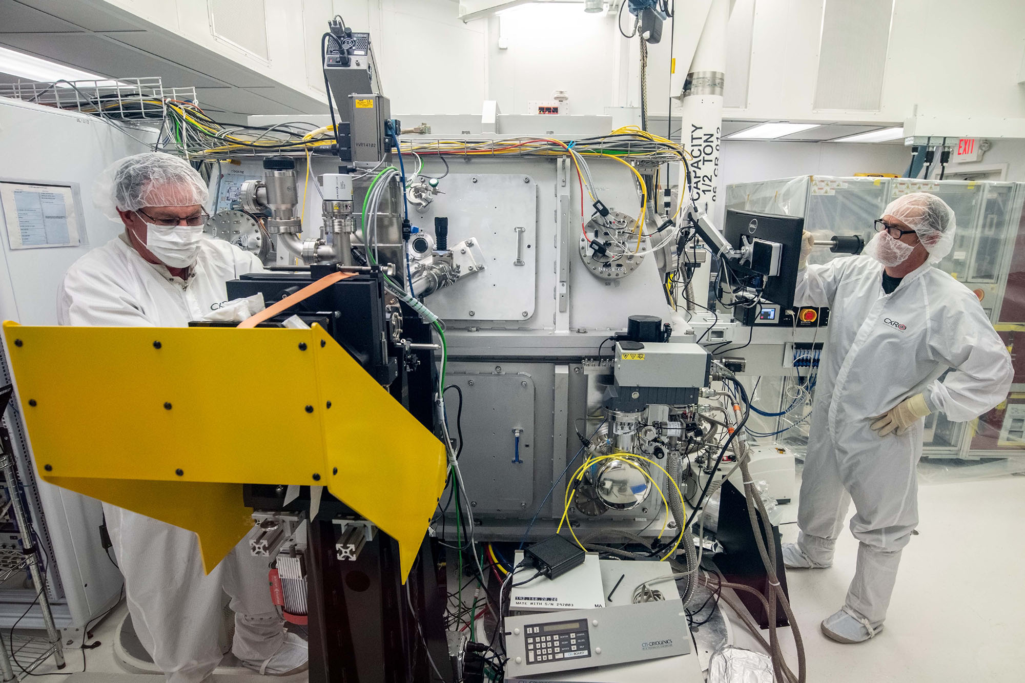
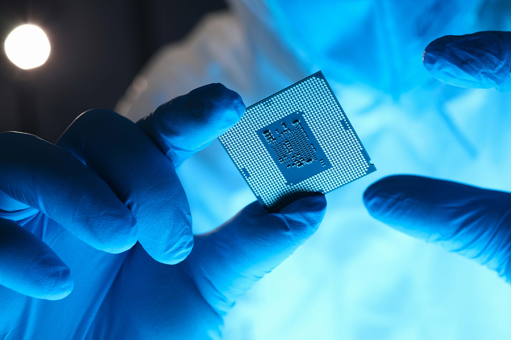
Bruno La Fontaine, director of the Center for X-Ray Optics and microelectronics expert, shares how advanced X-ray tools developed at the Lab are enabling breakthroughs in EUV lithography — an essential technology for printing smaller, faster, and more energy-efficient microchips. Learn how fundamental science at Berkeley Lab is shaping the future of devices we all rely on, from smartphones to the AI systems of tomorrow.
In this 7-minute audio interview, listen as Bruno La Fontaine, director of the Center for X-Ray Optics (CXRO), discusses how scientists at CXRO and the Advanced Light Source helped pioneer a revolutionary approach to making microchips called extreme ultraviolet lithography.
Early Research Demonstrated Novel Approach to Next-Generation Transistor Design
Compute This: Six Ways Berkeley Lab is Shaping the Future of Microelectronics
New Photon-Avalanching Nanoparticles Could Enable Next-Generation Optical Computers
Quantum Science
Frontier Computer Sciences
Materials and Chemical Sciences